CE Certified
 EN
 DE
 FR
 ES
 RU
 JA
Each module engineered directly on our factory floor in Dongguan, fully customized by dielectric stack-up, conductive ink conductivity, connector layout, and environmental IP rating.
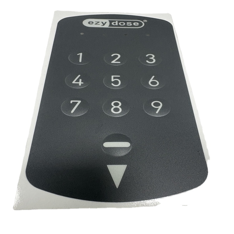
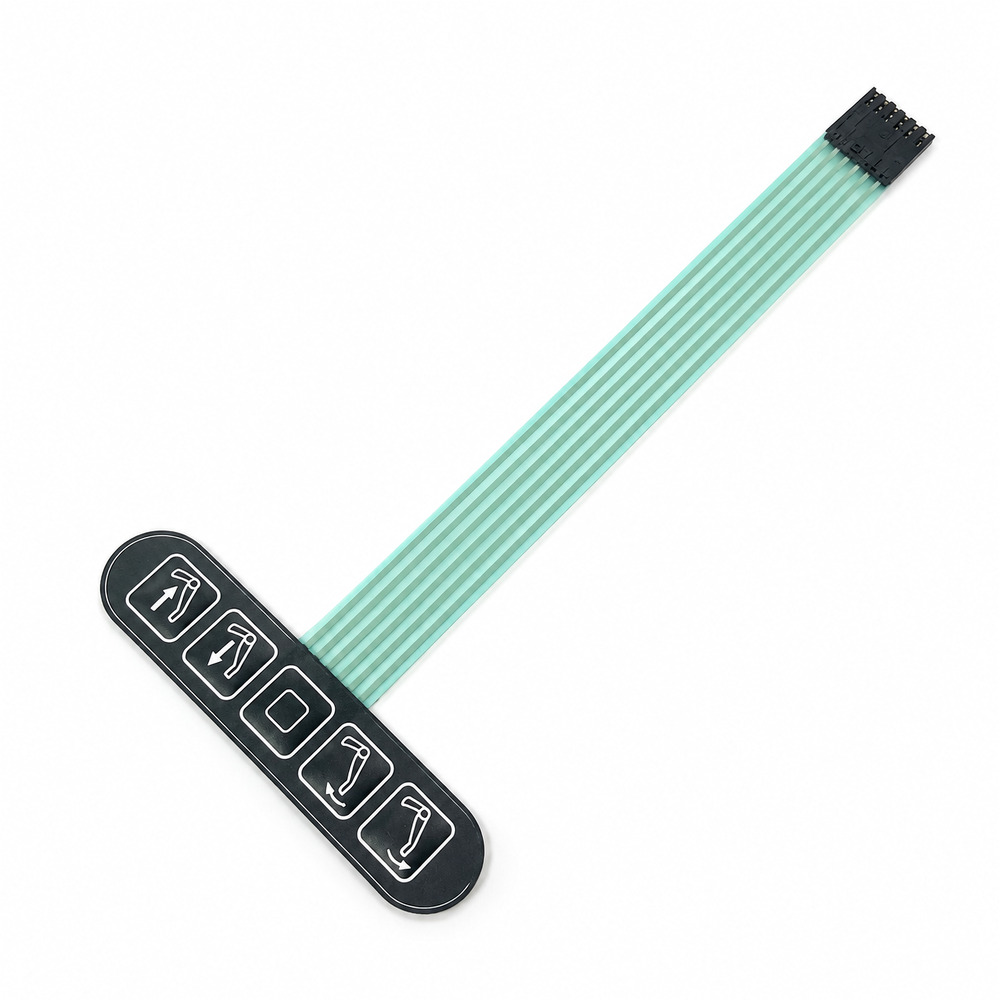
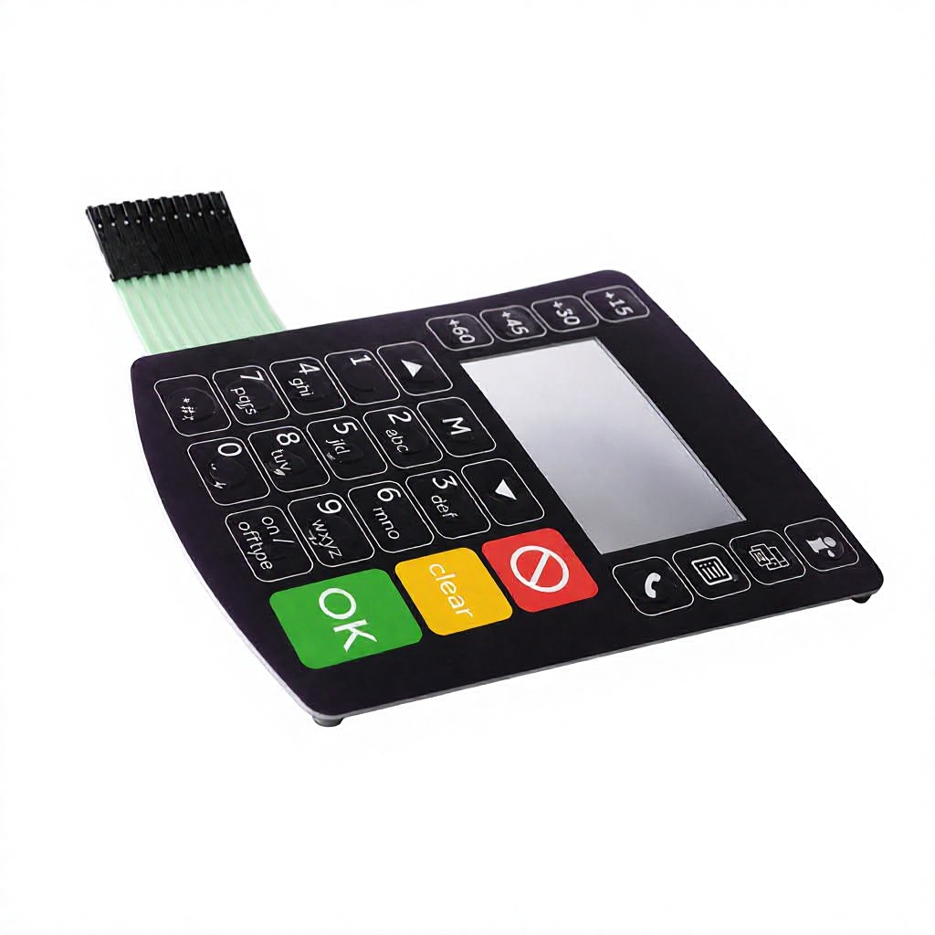
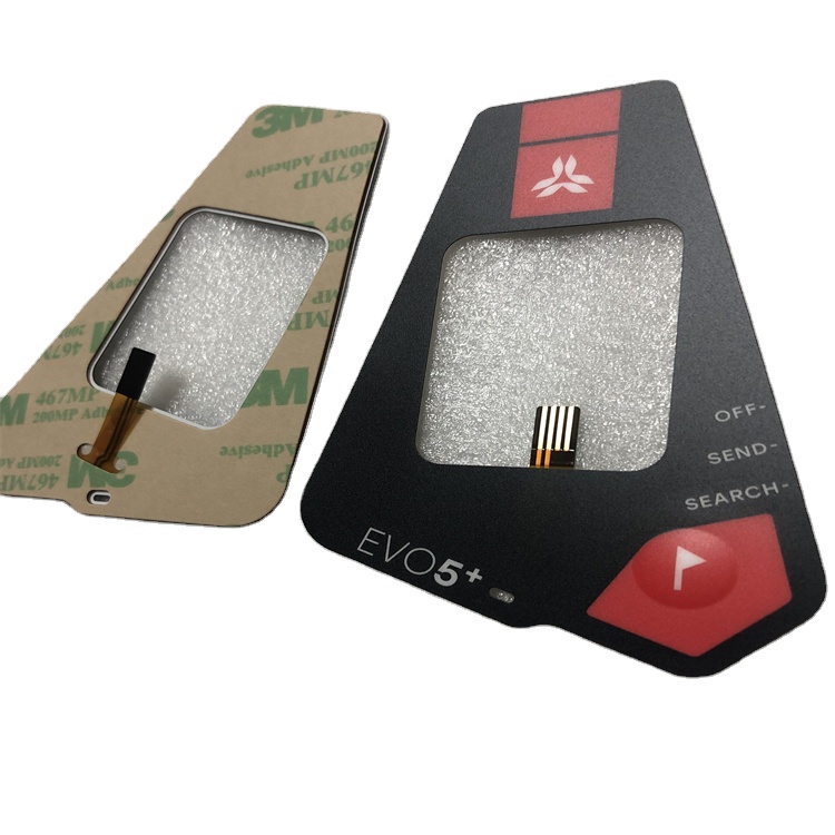
20+ years of dedicated precision HMI and conductive screen-print engineering.
Fully integrated die-making, lamination, cleanrooms, and testing facilities.
Direct factory technical review for mechanical and electrical layer design.
Full compliance testing for EN 61000-4-2 ESD and EN 61000-4-3 radiated immunity.
Capacitive touch sensing represents a massive shift from traditional mechanical switches to solid-state, zero-wear human-machine interfaces. However, achieving CE compliance under the Electromagnetic Compatibility (EMC) Directive 2014/30/EU presents significant design hurdles for global hardware exporters.
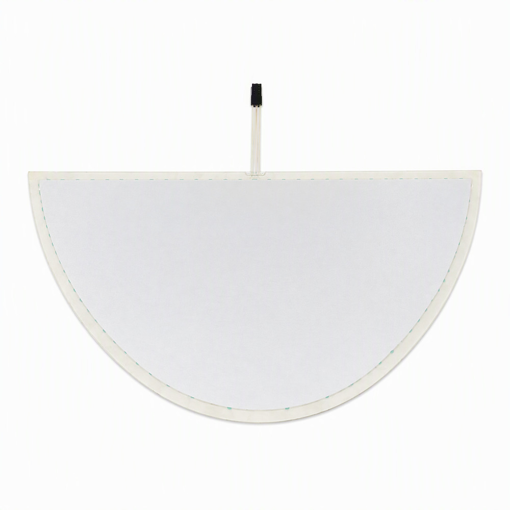
Projected Capacitance operates by scanning changes in charge distribution across an X-Y conductive matrix printed onto optical-grade polyester (PET) or polyimide (PI). When a conductive actuator—such as a human finger—approaches the dielectric overlay, it couples with the local fringing electric field, creating a parasitic capacitance to ground.
Our precision screen-printed silver micro-traces reduce trace resistance to under 10 Ω/cm, maximizing the Signal-to-Noise Ratio (SNR) and allowing touch detection through overlay cover panels up to 6.0 mm thick glass or 4.0 mm acrylic.
For equipment targeting European markets, capacitive touch sensors must satisfy rigorous electromagnetic immunity criteria without triggering false actuations or locking up. Industrial machinery requires compliance with EN 61000-6-2 (Immunity for Industrial Environments) and EN 55032 (Emissions).
Dongguan Ravo Electronics integrates dedicated ground-mesh shielding layers printed with low-impedance carbon-silver formulations. This boundary shunts fast transient bursts (EFT according to EN 61000-4-4) and radio-frequency radiated fields (EN 61000-4-3 up to 10 V/m) directly to chassis ground.
Changes in ambient relative humidity (RH) and temperature induce dielectric drift in low-cost sensor substrates, causing false touches or dead spots. Our engineering team utilizes heat-stabilized, biaxially oriented polyethylene terephthalate (PET) films with thermal shrinkage under 0.05% at 150°C for 30 minutes.
Paired with high-cohesion, optically clear laminating adhesives (OCA) from 3M (such as 3M 467MP, 468MP, or 8171P), our sensor stacks maintain stable dielectric constants (εr ≈ 3.0 to 3.4) across operating temperatures of -40°C to +85°C.
Optimizing capacitive sensor sensitivity begins with selecting the proper cover dielectric material and layer stack geometry. The table below illustrates standard material constants utilized in Ravo Electronics DFM engineering.
| Material / Layer Designation | Dielectric Constant (εr @ 1 MHz) | Typical Thickness Range | Transmittance / Clarity | Primary Industrial Application |
|---|---|---|---|---|
| Autotype Polyester (PET) Overlay | 3.1 – 3.3 | 0.125 mm – 0.250 mm | Textured / 89% (Clear) | Industrial HMIs, CNC Controllers, Food Processing Panels |
| Polycarbonate (PC) Hardcoat Sheet | 2.9 – 3.1 | 0.250 mm – 1.000 mm | Gloss/Matte / 90% | Medical Devices, Outdoor Vending, Transportation |
| Polymethyl Methacrylate (PMMA / Acrylic) | 3.4 – 3.7 | 1.000 mm – 4.000 mm | High Optical / 92% | Commercial Appliances, Laboratory Instrumentation |
| Chemically Strengthened Cover Glass | 6.8 – 7.2 | 1.100 mm – 6.000 mm | Ultra-Clear / >93% | Heavy Machinery, Marine Navigation, Rugged Military Gear |
| 3M 8171 / 8172 Optically Clear Adhesive | 3.3 – 3.5 | 0.050 mm – 0.125 mm | 100% Water Clear | Full Face Bubble-Free Lamination to Touch Substrate |
| Screen-Printed Silver Nanowire / Flake Layer | N/A (Conductive) | 0.010 mm – 0.018 mm | Opaque / Solid Pattern | Capacitive Button, Slider, and Matrix Electrode Arrays |
Global OEM sourcing directors are rapidly moving past generic commoditized switches. Procurement strategies are now shaped by 5 technological megatrends focused on smart functionality, tactile confirmation, and resilience.
Traditional capacitive sensors suffer from false triggers when subjected to conductive fluids like water droplets, saline mist, or oil films. Next-generation procurement frameworks demand mutual capacitance sensing architecture with dynamic driven-shield layers.
By printing active out-of-phase guard rings around touch pads, our factory cancels out false capacitance shifts caused by pooling liquids, ensuring 100% reliable operation for kitchen ovens, dialysis equipment, and outdoor maritime consoles.
The market is shifting rapidly from flat 2D panels to ergonomic, organically curved surfaces. In-Mold Electronics (IME) integrates conductive traces, SMD capacitive ICs, and LEDs directly into a single thermoformed and injection-molded structural plastic shell.
This reduces assembly part counts by up to 70%, sheds significant weight in automotive cockpits and handheld medical devices, and eliminates mechanical gaps where dust and moisture accumulate.
One inherent challenge of flat capacitive surfaces is the lack of tactile feedback, which can cause operators to look down from critical tasks. Modern procurement specifications increasingly call for combined Capacitive + Force Sensing Resistor (FSR) stacks.
The circuit requires both a capacitive touch proximity match and a definite mechanical pressure threshold (typically 1.5N to 3.0N) to execute the command, backed by miniature resonant actuator haptic buzzes—preventing catastrophic accidental triggering in aerospace and surgical HMIs.
Industrial assembly lines, cold storage distribution centers, and emergency response crews require technicians to wear heavy latex, nitrile, leather, or synthetic thermal gloves. Thick gloves increase the distance between the skin dielectric and the sensor plane, degrading the sensing charge.
Our engineers implement high-sensitivity multi-stage amplification firmware paired with customized electrode pitch designs, ensuring responsive activation through 5 mm insulated winter or electrical safety gloves.
Tier-1 OEM buyers are shedding fragmented supply chains that separate screen-printers, circuit etchers, and injection molders. Modern sourcing teams demand single-source suppliers like Dongguan Ravo Electronics that control everything under one roof.
From tooling and screen production to laser micro-machining, automated SMD component mounting, cleanroom optical bonding, and strict compliance with RoHS, REACH, and Conflict Minerals declarations, we streamline the entire manufacturing lifecycle.
Founded in Fenggang Town, Dongguan—the epicenter of South China's high-precision electronics manufacturing corridor—Dongguan Ravo Electronics Co., Ltd. has developed from an 8-person engineering workshop in 2003 into an industry-leading 12,000 m² cleanroom manufacturing plant.
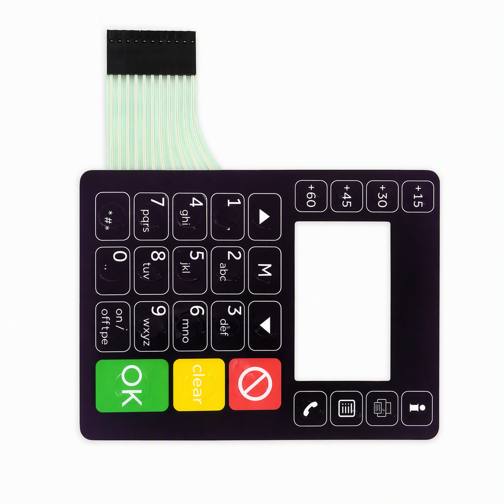
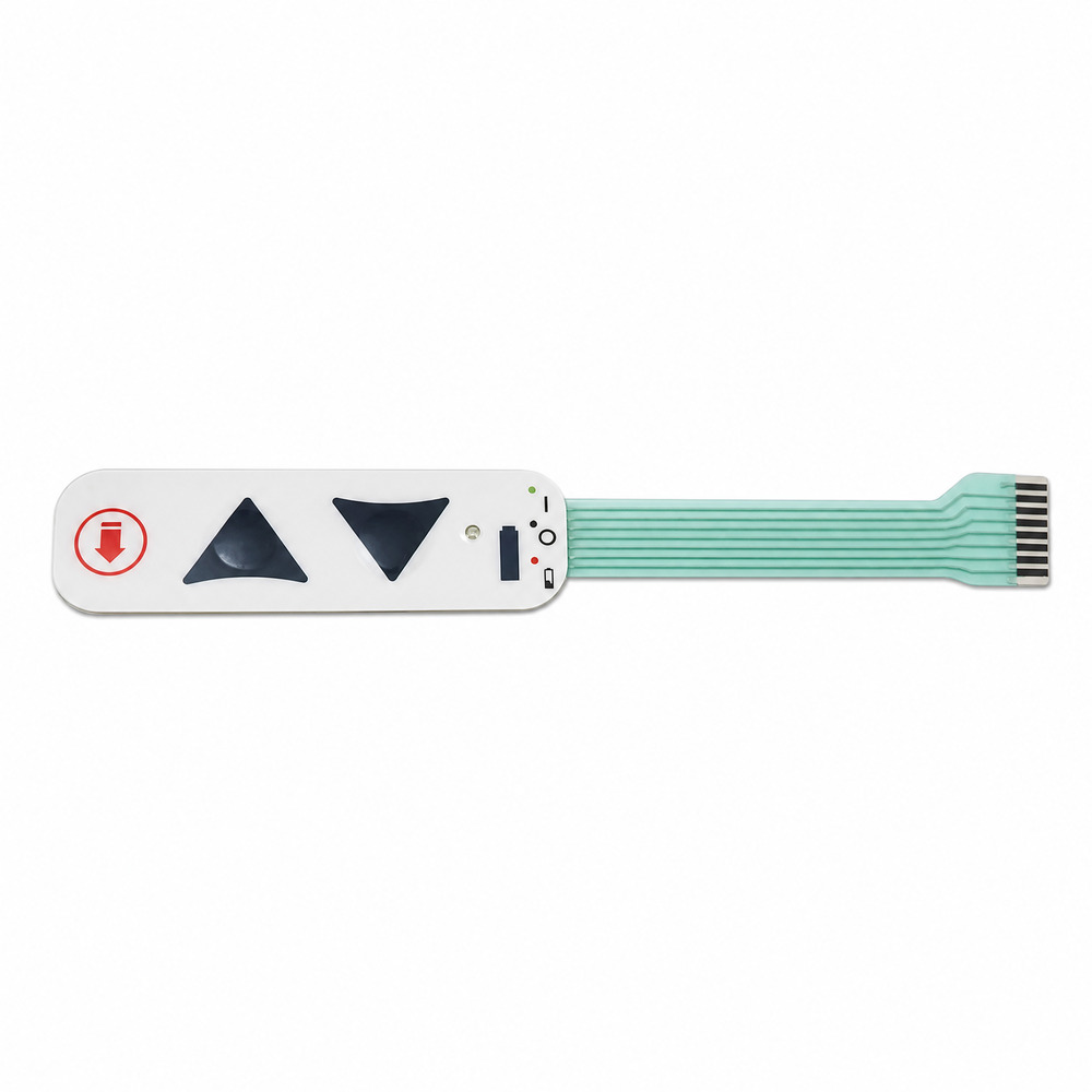
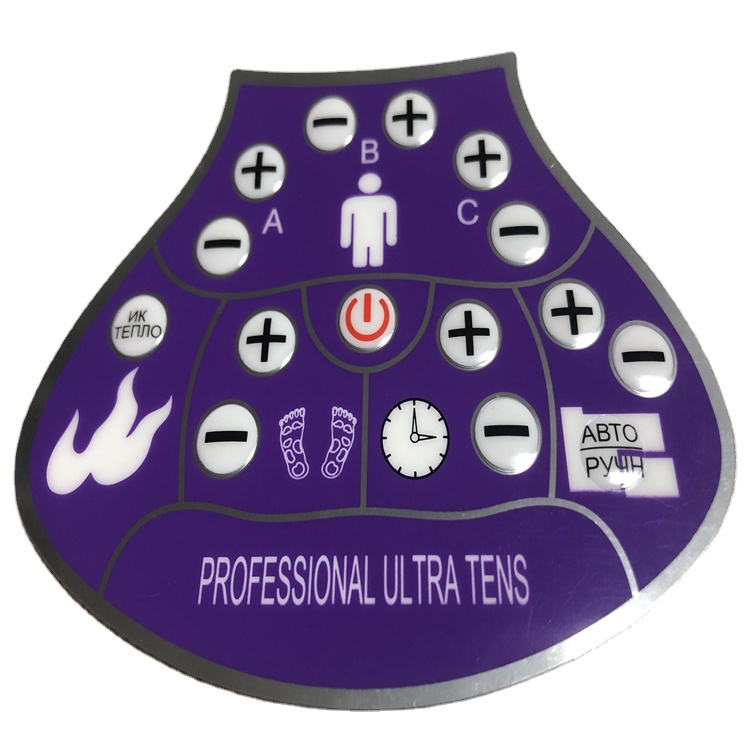
We specialize in custom membrane switches, capacitive touch sensors, graphic overlays, flexible printed circuits (FPC), rigid FR-4 PCB assemblies, silicone rubber keypads, and thin-film force sensitive resistors (FSR). By housing mold design, tooling, conductive paste screen printing, laser die-cutting, optical bonding, and environmental testing entirely within our Fenggang facility, we eliminate multi-tier subcontractor markups and quality drift.
Whether your program demands a 1-piece rapid prototype for proof-of-concept functional validation or a high-volume run of 500,000 units with automated optical inspection (AOI), our engineering team provides full Design for Manufacturability (DFM) reviews within 2 business hours.
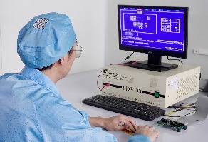 Main Production Floor
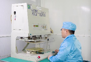 Class 1,000 Cleanroom
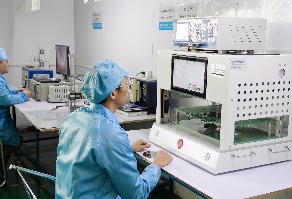 Multi-Layer Lamination
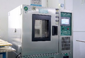 100% Electrical Inspection
Detailed answers to common design, compliance, material, and testing questions encountered when ordering custom capacitive touch sensors from China.
Our CE declaration is verified through formal testing in accredited third-party laboratories (including SGS and TÜV testing regimes). We certify compliance with the EMC Directive 2014/30/EU covering EN 61000-4-2 (Electrostatic Discharge Immunity up to ±15 kV air / ±8 kV contact discharge), EN 61000-4-3 (Radiated RF Electromagnetic Field Immunity up to 10 V/m), and EN 61000-4-6 (Conducted Disturbances). Full test certificates, material RoHS declarations, and REACH chemical reports accompany first-article submission packages.
We implement a dual-layer engineering strategy. Mechanically, we design active shielding circuits—a continuous or cross-hatched screen-printed guard ring that surrounds individual electrodes and tracks, held at the same electrical potential as the sensing pad. Digitally, we match trace geometry to modern controller IC firmware (such as Microchip, Cypress, or Azoteq) using mutual-capacitance matrix algorithms that detect the localized dip caused by a grounded human finger while discarding uniform water films.
To deliver an actionable DFM within our standard ≤ 2-hour window, please provide: (1) Mechanical CAD drawings in DXF, DWG, or STEP format showing outer dimensions, cutouts, and tail exit location; (2) Graphic artwork in Adobe Illustrator (.AI), CorelDRAW, or vector PDF with exact Pantone (PMS) or RAL color codes specified; (3) Schematic or pinout requirements including connector pitch (e.g., 2.54 mm, 1.0 mm, or 0.5 mm ZIF); (4) Desired cover overlay material, thickness, and operating environment parameters.
Yes. We utilize three primary illumination architectures depending on profile limits: ultra-thin Light Guide Films (LGF) with side-firing SMD LEDs (total thickness as slim as 0.8 mm to 1.2 mm), embedded thin-profile SMD LEDs with proprietary light-diffusing spacer layers, or uniform dead-front masking where icons remain completely invisible until illuminated. Our optical team balances lumen output and color balance to eliminate hotspots across buttons and sliders.
We support development agility by offering prototype batches starting from just 1 to 10 pieces. For volume production, standard order sizes typically range between 500 and 10,000+ pieces. After drawing and artwork sign-off, standard functional prototypes are manufactured and shipped within 7 to 12 working days. High-volume production batches typically ship within 3 to 4 weeks depending on component sourcing and automated assembly requirements.
Silver migration occurs when moisture combines with DC voltage potential across adjacent silver traces, causing dendritic silver growth and short circuits. Ravo mitigates this risk by: (1) Applying an overlapping, high-density carbon paste or hydrophobic dielectric encapsulation ink over all silver printed traces; (2) Maintaining minimum spacing rules (>0.5 mm between critical voltage lines); (3) Utilizing hermetically sealed 3M perimeter adhesive gaskets rated to IP67/IP68.
We support a variety of interconnect systems: standard 2.54 mm pitch female crimp connectors (Amphenol, Nicomatic, FCI Clincher) with locking housings; fine-pitch (1.0 mm or 0.5 mm) heat-bonded polyimide FPC tails compatible with zero-insertion-force (ZIF) board sockets; or directly soldered wire harnesses. For ZIF tails, we laminate localized FR-4 or polyimide stiffeners to guarantee precise insertion contact force and pull-out resistance.
Every single capacitive touch and membrane switch batch undergoes 100% automated electrical continuity, resistance, and insulation breakdown testing on computer-controlled test fixtures. In addition, we perform optical window clarity validation, spectrophotometer color delta (ΔE) verification against approved Pantone targets, overlay cross-hatch adhesion testing (ASTM D3359), and cycle life testing on sample units to verify 5,000,000+ touch actuations without performance degradation.
